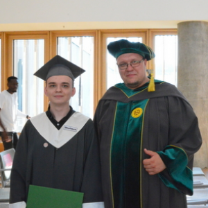
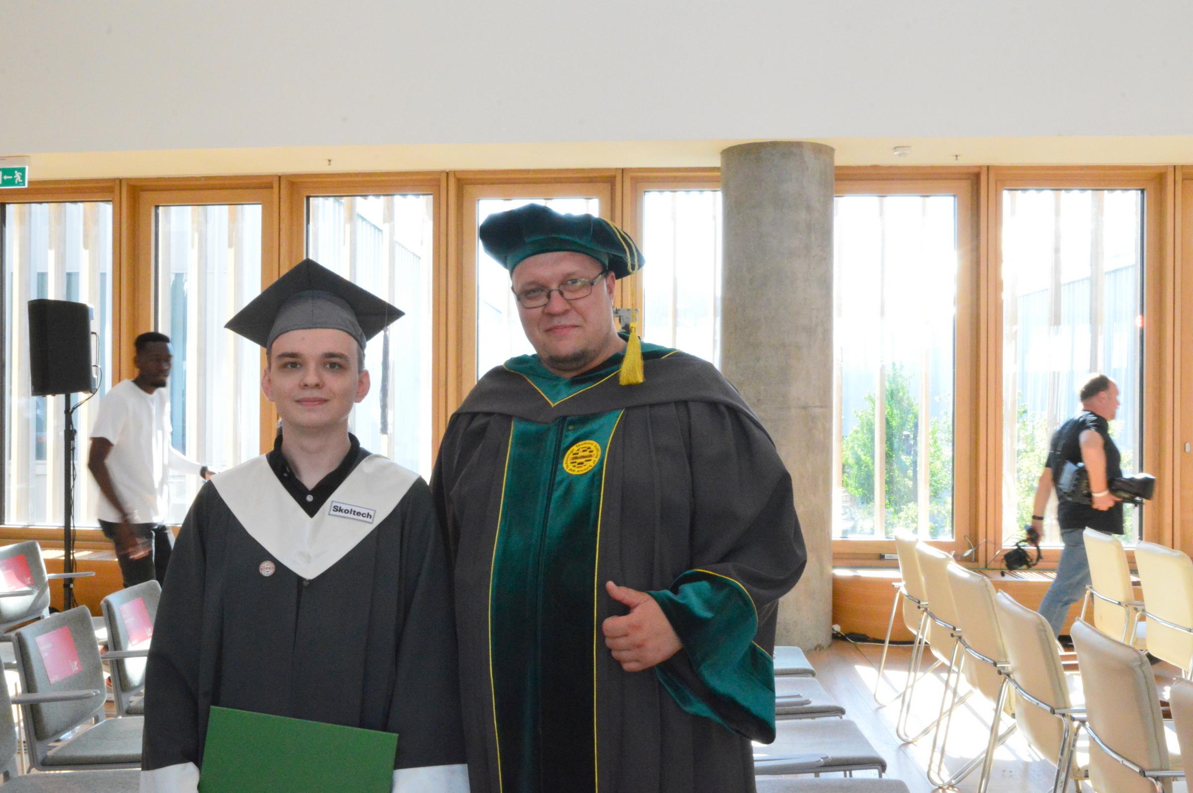
In 2024, Kirill Malgin completed his Master's degree at the Skolkovo Institute of Science and Technology and became the first graduate of the Double Degree program at Samara University and Skoltech. Now he is going to post-graduate school there, in Moscow, to continue his research.
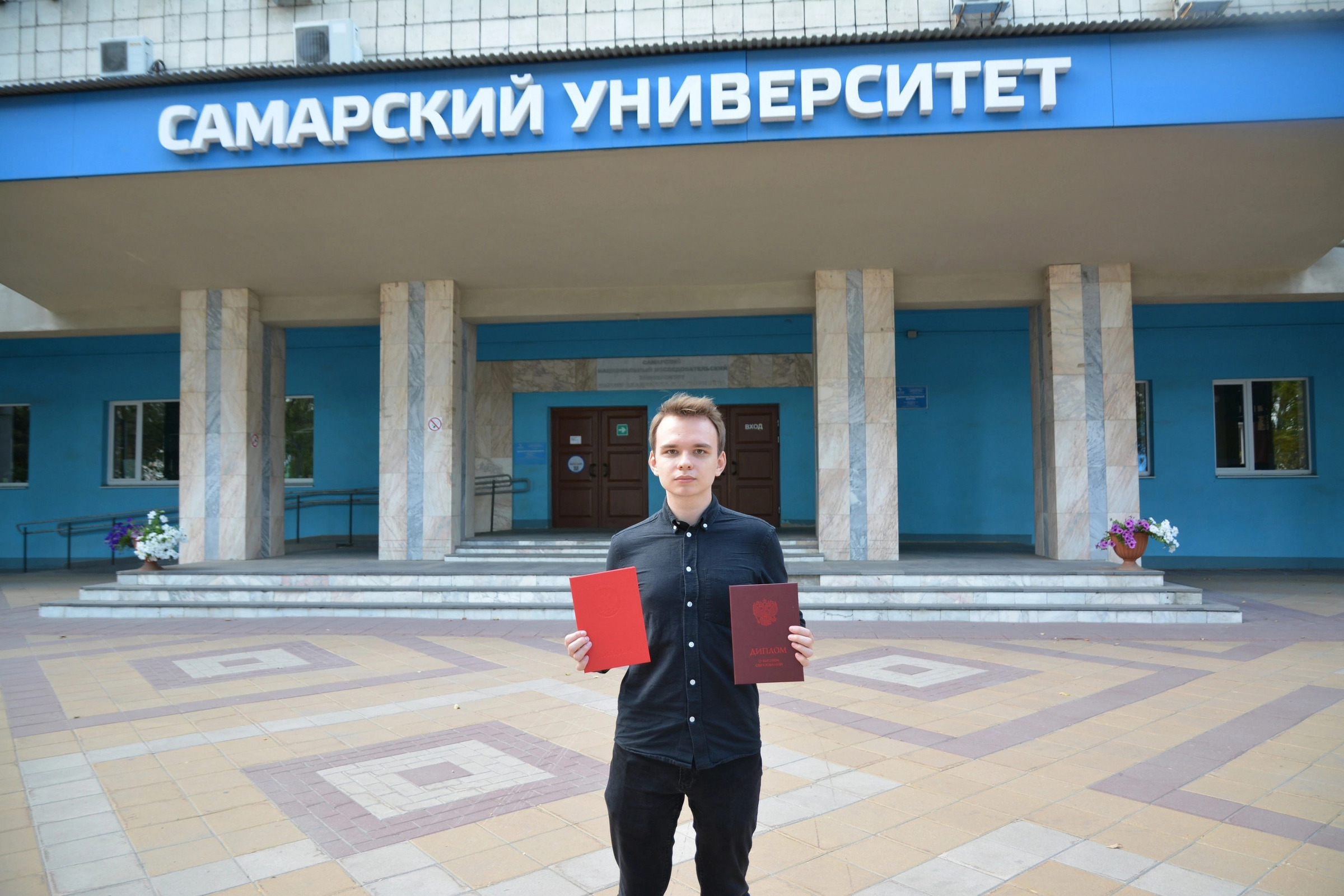
Kirill Malgin graduated from school in Dimitrovgrad, passed the Unified State Exam in physics and computer science and chose to enter between the universities of Ulyanovsk, Samara and Kazan. "I found the right specialty only at Samara National Research University. Studying possible areas, I fluctuated between theoretical physics, electronics and nanoelectronics, and nanoengineering. The magical effect of the "nano-" prefix worked, and I enrolled in electronics and nanoelectronics. Subsequently, I realized that I was not mistaken in my choice," Kirill admitted.
The young man did not come to science immediately. For the first two years, he focused only on his studies. But from the third year special courses began, they talked about the final qualifying work, and Kirill asked associate professor of the Department of Nanoengineering Alexei Arkhipov to act as his supervisor.
"I knew Alexey Vladimirovich from the first year: he taught material science, then the basics of technology, the design of an electronic component base," Kirill Malgin told. The thesis was devoted to the development of a method for diagnosing electrodiffusion failures of microcircuits.
"When current flows through the electrical network, the mass of a conductive substance is transferred from one place to another. And defects arise. That is, the conductive paths become narrower in some places, and wider in others. Where the "manifold" narrows, the current density increases, at some point this part of the chip overheats, and a rupture occurs," explains Kirill. The bachelor's task was to develop a methodology that would allow predicting such gaps. And Kirill suggested using thermochromic liquid crystals which change their color when heated. “We selected a liquid crystal mixture, a solvent for it and a method of application. This is the case when you are conducting a new study for which there are no sources yet. So it wasn't easy," the young scientist recalls.
Kirill was so captivated by science that he did not hesitate to choose a Master's degree from Samara University. The newly minted graduates were invited by the head of the Department of Nanoengineering, Professor Vladimir Paveliev, to try their hand at the master's double degree program of Samara University and Skoltech "Photonics and Quantum Materials". Kirill Malgin passed the selection, received a scholarship in the amount of 40 thousand rubles per month and went to Moscow.
"The educational process at Skoltech is entirely in English. Thanks to Svetlana Avdeiko, my English teacher at Samara University. Thanks in large part to her lectures, my language skills allowed me to integrate into the educational process without any problems. It was easier to communicate with classmates, understand lectures, and do homework," Kirill notes. By the way, there are few homework assignments in Skolkovo. They believe that this allows you to focus on research.
The education system in Skolkovo is based on individual educational trajectories. To complete the training, you need to collect a certain number of credit units that you receive for the courses you have attended. The credits are divided into sections of the courses: the main part is the core of compulsory subjects, research, entrepreneurial and optional.
"I had two compulsory courses: quantum mechanics and fundamentals of photonics. From the optional section, I chose a course on 3D modeling in CAD systems. I was very interested in courses related to carbon nanomaterials, aerosol technologies, and catalysis. The first two were taught by Albert Nasibulin, a specialist in the field of synthesis, research on growth mechanisms and the use of nanomaterials. He became my scientific supervisor from Skoltech. Catalysis was taught by Dmitry Krasnikov, who was my co-supervisor. At Samara University, I studied courses in surface physics and engineering entrepreneurship," Kirill Malgin told about the details.
The Master's degree in the field of Photonics and Quantum Materials proved the continuity of the educational programs of the two universities.
"Many subjects that I studied at Samara University were useful in the Skolkovo Master's program. Mathematics, the basic subject that Mark Nechaevsky taught us, made life very much easier for me at Skolkovo. I am grateful to him both for his knowledge of mathematical analysis, linear algebra, and for the wise thoughts that he shared not only on the subject — he passed on his experience to us. Subjects such as vacuum engineering, courses in quantum computers and static applied quantum mechanics have also become useful. You're sitting at a lecture in Skolkovo and you understand: “It's already happened!” Kirill Malgin says. “The skills of working with such complex research equipment as the atomic force microscope which we received in our Bachelor's degree helped us a lot. This is a fairly powerful diagnostic tool that allows you to consider the relief of the material. Depending on the modifications of the microscope, you can learn about the electrical properties of the material."
During his Master's degree, Kirill developed a method for synthesizing perforated graphene using the Boudoir reaction. The scope of graphene application is extensive. The most common is as an element of systems from which heat must be quickly removed, since graphene is characterized by high thermal conductivity. Perforated graphene is potentially applicable in transistors, quantum cascade lasers, optical absorbers and photonic crystals. But it depends on the configuration of the sample: the perforations in the film may be more ordered or less. If they are less ordered, then the scope of application is narrowed, and the results will not be highly accurate. In the graphene synthesized by Kirill, the perforation is not ordered and is the same in shape. But such a material can also be used in gas or biosensors.
"The results are inspiring. We studied the samples obtained through an optical microscope, a scanning electron microscope and an atomic force microscope. Indeed, everything looks exciting. It is interesting to analyze how my ideas have been realized,” says Kirill. “In post-graduate school, I want to continue experiments. There are ideas on how to make the perforation more orderly. Yes, perforation ordering methods already exist, but we want to find a new technology so that the result is competitive." In post-graduate school, the young man will look for options for using perforated graphene in devices for physical research.
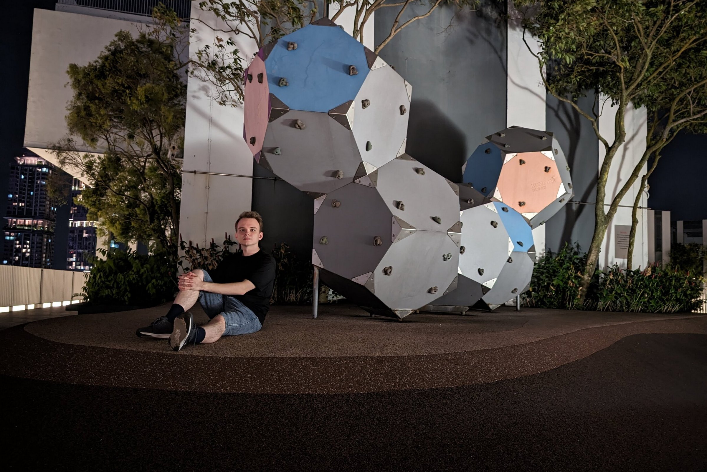
One of the opportunities to study at Skoltech is to work on joint projects with other universities in Russia and abroad. Graduates regularly go on internships in St. Petersburg, Harbin. In the spring, Kirill completed an internship in Singapore, where he conducted experiments with the resulting samples of perforated graphene.
"In Singapore, we conducted experiments on growing amorphous carbon in graphene film perforations. I prepared samples of perforated graphene at Skoltech, and the cultivation of amorphous carbon took place at the National University of Singapore. The results were successful. This could potentially reveal interesting physical properties of such samples. I plan to continue experiments on this topic already in post-graduate school at Skoltech and go back to Singapore to scientific partners," Kirill Malgin concluded.
Photos provided by the hero of the publication